Email:
sales@hypersolidmetal.comWhatsapp:
8618625975081
Email:
sales@hypersolidmetal.comWhatsapp:
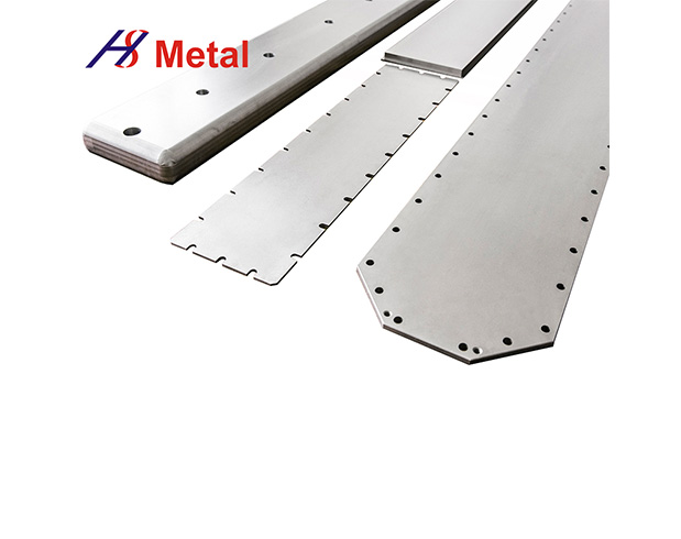
8618625975081Sputtering targets are used to prepare thin film materials in integrated circuits through the magnetron sputtering process and are widely used in key components such as wafer conductive layers, barrier layers, and metal gates. In different technology nodes, metal targets such as aluminum, copper, titanium, and tantalum play differentiated roles according to their characteristics and process requirements. Aluminum targets are still widely used as wiring materials in technology nodes above 110nm, while copper targets have become the mainstream choice in advanced processes below 110nm, and tantalum targets are used as barrier layer materials for copper wiring.
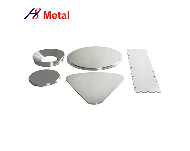
Metal sputtering targets for integrated circuits include a variety of high-purity metals, which are used in combination at different technology nodes to meet the needs of logic chips, memory chips, and high-performance, low-power devices. With the advancement of Moore’s Law, the technical requirements for sputtering targets continue to increase, and the research and development direction has shifted to the collaborative design of multi-material systems.
In general, as a key link in the integrated circuit industry chain, the technological evolution of sputtering targets is closely linked to changes in market demand. As the global semiconductor industry moves towards smaller processes and higher performance, the material system and process adaptability of sputtering targets will become important factors in determining the competitiveness of the industry.
With the continuous development of large-scale and very large-scale integrated circuit (VLSI) technology, the integration of integrated circuits is getting higher and higher, the feature size is getting smaller and smaller, and the performance requirements for metal sputtering targets are becoming increasingly stringent.
In the future, the development of metal sputtering targets will show the following trends:
First, the purity of the target will be further improved to meet the needs of finer micron and nano processes, and the purity requirement will reach 6N and above; second, the target will develop in the direction of large size to adapt to the trend of wafer size gradually developing towards 450mm, thereby improving production efficiency and material utilization; finally, the grain size of the target will be further reduced, and the uniformity of the organization will be further improved to ensure the uniformity and high quality of thin film deposition, especially in the filling of high aspect ratio trenches.
These trends will promote the continuous innovation of metal sputtering target technology to meet the rapid development needs of emerging fields such as artificial intelligence chips, cloud computing, and smart cars.