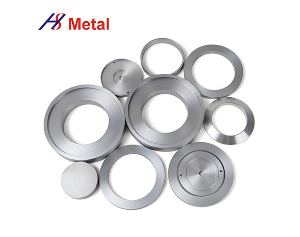
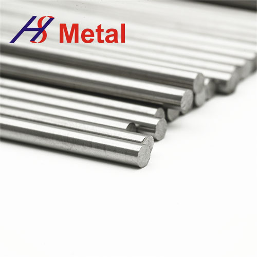
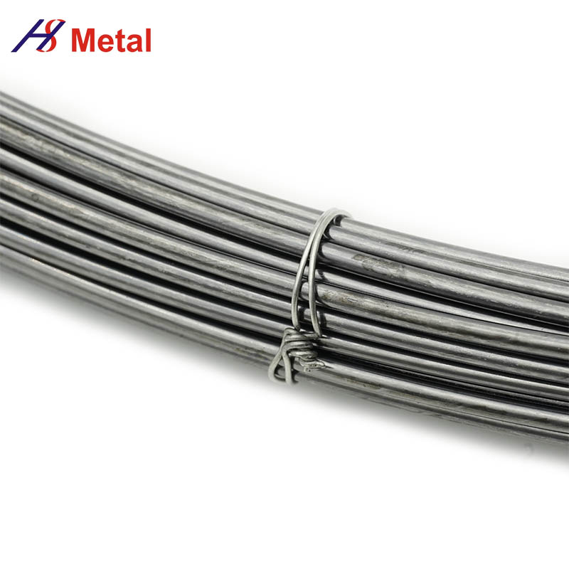
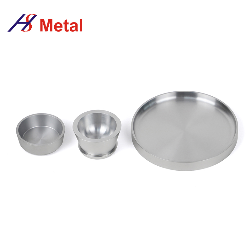
Molybdenum wire standards and grades
Molybdenum wire features a high melting point, high strength and elastic modulus, a low coefficient of expansion, low vapor pressure, excellent electrical and thermal conductivity, and corrosion resistance. It is widely used in lighting, vacuum devices, machining, and spray coating applications. Molybdenum wire standards provide comprehensive regulations for its quality, specifications, production, and applications, representing the technological level of molybdenum wire production. China’s earliest molybdenum wire standard was SJ316-72, “Molybdenum Wire,” in 1972. Following improvements in molybdenum wire production technology, GB4182-84 “Molybdenum Wire” was released 12 years later, and T4182-1997 “Molybdenum Wire” was released 15 years later. The currently commonly used standard is GB/T4182-1997 “Molybdenum Wire.” US molybdenum wire standards are categorized into coarse and fine wires, defined by ASTM F 289 and ASTM B 289. ASTM F 289 was developed in 1954 and first published as ASTM B289-54 T. It was revised again two years later and re-established as ASTM F 289-56. Twenty-five years later, it was revised as ASTM F 289-81, and 15 years later, it was revised again and published as ASTM F 289-96. The current standard is ASTM F 289-96. ASTM B 387 was first published in 1962, with the original version being ASTM B687-62 T....
2025-08-29
Learn More